Eagle PCB -> LPKF Milling Machine Micro-How-To
Instructions for users in EEE, University of Nottingham
EAGLE 4.09rl (Linux) CircuitCAM 3.0 (99) and BoardMaster 3.0 (45)
Steve D. Sharples
This is the short version, explaining giving only brief details. If
you want the full procedure step-by-step, please go to the
Full EAGLE Export Page.
1. SPECIFIC ISSUES TO EEE
1a. Design rules
- once you have "created a board from schematic", click on the "DRU" button
- a window will pop up, it will probably say "EAGLE Design Rules"
- click on the "Load" button
- navigate your way to the following directory: /home/share/eagle/local_dru/
- double-click on "steve.dru" (right click to download)
- click on "Ok"
1b. Extra layers (for the milling machine)
It is important to follow the following conventions,
otherwise your boards may not be exported and manufactured correctly
Layer conventions used
| Layer | Name | Colour | There by default? | Used for... |
| 41 | tRestrict | Diagonal red stripes | Yes | Areas on Top layer
that you wish to be completely milled out except for tracks, pads and vias |
| 42 | bRestrict | Diagonal blue stripes | Yes | Areas on Bottom layer
that you wish to be completely milled out except for tracks, pads and vias |
| 117 | tText | Usually white | No | For text on Top layer... will be
milled out with 0.2mm cutter |
| 118 | bText | Usually white | No | For text on Bottom layer... will be
milled out with 0.2mm cutter |
1c. Shared files in Eagle: /home/share/eagle/
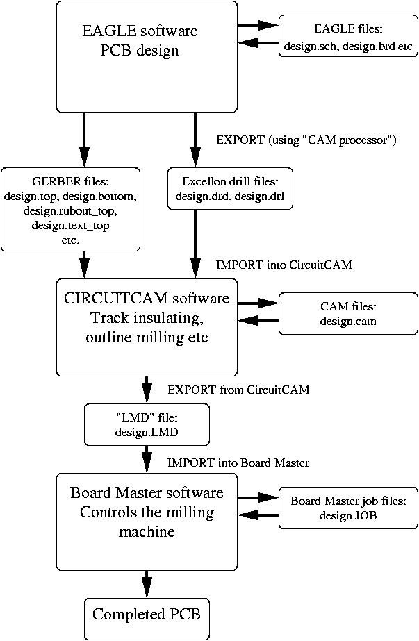
2. THE EXPORT/IMPORT PROCEDURE OVERVIEW

3. EXPORTING FILES FROM EAGLE
- in the "Board" window, type: run drillcfg
- a window pops up, asking for units... default is mm, select INCH.
- in the "Board" window, click on the "CAM" icon (next to the printer icon)
- click File -> Open -> Job...
- double-click "EEE_milling.cam" (right click to download)
- click "Process Job"
- open up a "konsole"/"shell" window
- put a floppy disc in the disc drive
- change to the directory where your files are stored, eg:
cd ~/eagle/my_current_design/
- type: eagle2floppy
- once told to do so, remove the disc from the drive
4. IMPORTING THE FILES INTO CIRCUITCAM
4a. The Gerber Files (Top, Bottom and BoardOutline etc)
- Import (eg) "design.bottom"
- in the "Aperture/Tool list" box, type "bottom" (or something)
- Select "Bottom Layer"
- etc...
4b. The Excellon Drill Data
- Import "design.drl"
- select "Eagle_Excellon.txt" from the "Aperture/Tool Template" list
- in the "Aperture/Tool list" box, type "drills" (or something)... "Ok"
- Import "design.drd"
- in the "Aperture/Tool list" box, SELECT "drills" FROM THE LIST
- Select "DrillPlated" (or DrillUnplated for single-sided boards) layer...
click "Ok"
5. INSULATING THE COPPER
- click Edit -> Insulate... select "Bottom layer"... click "Run"
- click Edit -> Insulate... select "Top layer"... click "Run"
6. BOARD CUT-OUT
- click Edit -> Contour Routing...
- select the whole of the BoardOutline layer, and ERASE this layer
- click near the grey CuttingOutside rectangle to select it
- use the "+" and "-" keys on the keypad to move the "*" around the
rectangle
- press "Ctrl-g" to make a gap in the middle of one side. Do same on other side
7. SAVING AND EXPORTING
- save as "design.cam" ... MAXIMUM 8 LETTERS (BoardMaster is very old)
- click File -> Export -> LPKF CircuitBoardPlotter... saves "design.LMD"
8. IMPORTING BOARD INTO BOARDMASTER
- File -> Import -> LMD/LPR...
- select your file "design.LMD"
- check everything's there and ok (view both sides, select "Real Tools"
etc)
Feel free to modify, redistribute etc under the terms of the GNU Public License
Hope it's useful!

