Difference between revisions of "Hamed Pezeshki"
(→PhD student, Faculty of Engineering, Department of Electrical and Electronic Engineering) |
|||
| Line 29: | Line 29: | ||
'''Publications:''' [https://scholar.google.co.uk/citations?user=eJiSUHkAAAAJ&hl=en View my profile on Google Scholar] | '''Publications:''' [https://scholar.google.co.uk/citations?user=eJiSUHkAAAAJ&hl=en View my profile on Google Scholar] | ||
| − | '''Get more information about me at:''' [https://www.linkedin.com/in/hamed-pezeshki-9502756b View my profile on Linkedin] | + | '''Get more information about me at:''' |
| + | *:[https://www.linkedin.com/in/hamed-pezeshki-9502756b View my profile on Linkedin] | ||
| + | |||
| + | *:ORCID iD: https://orcid.org/0000-0001-8252-0525 | ||
| + | |||
| + | [[File:Hamed_Pezeshki_ORCID.png]] | ||
'''Email:''' hamed.pezeshki@nottingham.ac.uk | '''Email:''' hamed.pezeshki@nottingham.ac.uk | ||
Latest revision as of 11:53, 26 July 2019
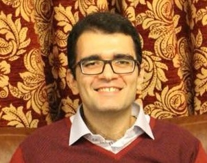
Hamed Pezeshki
PhD student, Faculty of Engineering, Department of Electrical and Electronic Engineering
Hamed Pezeshki is a PhD student at the University of Nottingham and has started his studies from Dec. 2016.
His research is about design and fabrication of waveguide-coupled devices for biosensing applications including optically sensing, trapping, and manipulating of nanoparticles and single molecules.
He has been qualified to be awarded by “Faculty of Engineering Research Excellence PhD Scholarship”, for his course of study.
He also has been awarded the “Preparing to Teach in Higher Education Certificate” from Professional Development at the University of Nottingham.
His area of expertise includes:
- Photonic crystal microcavities.
- Add/drop optical multichannel filters based on photonic crystals.
- All-optical bistable switches and gates based on photonic crystals.
- Localised surface plasmon resonance based nano- and micro-antennas.
- Polarization conversion based on plasmonic antennas.
- Silicon-on-insulator (SOI) semiconductor waveguides.
- Silicon nitride (Si3N4) dielectric waveguides.
Publications: View my profile on Google Scholar
Get more information about me at:
- ORCID iD: https://orcid.org/0000-0001-8252-0525
Email: hamed.pezeshki@nottingham.ac.uk
Location:
Room 1004, Tower Building,
The University of Nottingham,
University Park,
Nottingham,
NG7 2RD

