Finlay Nelson
Electro-optical imaging of cancer: Nanoscale impedimetry
It has been widely recognised that the electrical properties of cells dictate their function, and that the effects of drugs and disease are reflected in changes to these properties. The principal aim of this project is to exploit the intimate relationship that exists between the optical and electrical properties of plasmonic materials for voltage sensing and impedance imaging applications. It is expected that through careful observation and manipulation of this relationship that a label-free optical technique can be established by which to measure the electrical properties of biological samples with < 1μm spatial resolutions otherwise unattainable using existing technologies. The form of impedance micro-spectroscopy that is the focus of this research will consequently, through optical interrogation of high-bandwidth electrical impedance, allow the faithful reconstruction of highly local equivalent electrical networks that accurately describe spatially heterogeneous biological systems. With this information it will be possible to garner valuable insight into the mechanisms underpinning the function of healthy and pathological cells alike, and thereby provide a pathway to better understanding disease at the micro-scale.
Supervision
- Sidahmed Abayzeed (primary)
- George Gordon
- Richard Smith
- Rafael Fuentes-Dominguez
- Matt Clark
Inverse Mie Modelling
Based on a Drude interpretation of electrical conduction, the effects of charge on the optical properties of plasmonic nanostructures are confined, through electrostatic screening effects, to only their very peripheries. Within the so-called Thomas-Fermi screening length, metals exhibit drastically different permittivities than found in the bulk, but penetrating typically less than a single Angstrom into the metal its effects on the structure as a whole are usually negligible. However, when considering plasmonic nanostructures, who’s dimensions are no more than a few hundreds of nanometres, these charge-dependent effects become far more significant. It is extremely useful, therefore, to be armed with prior knowledge of the optical properties of a proposed nanostructure morphology. This task, while usually allocated to numerical simulation using finite element models, becomes exceedingly problematic in the case of charged nanostructures owing to the dimensions of the Thomas-Fermi screening length. One facet of this work is therefore to develop an alternative approach to modelling the optical response of charged nanostructures based on effective medium theory.
This branch of material science is concerned with describing complex composite materials with heterogeneous properties as homogeneous equivalents. In this particular application we therefore replace the material within the Thomas-Fermi domain and a portion of the adjacent bulk, with a larger artificial domain of uniform permittivity that accurately reflects the behaviour of the original system. Charge-dependent effects are thus preserved within this new description, but importantly by virtue of its increased thickness such a domain can be easily described in finite element models. While there already exist effective medium approximations for will dispersed mixtures, the applicability of these to charged nanostructures remains in question and so a more robust method is being investigated, beginning with an inverse approach to Mie theory. Traditionally Mie theory is used to ascertain the optical properties (scattering, absorption, etc.) of particles, specifically spheres, whose diameter is in the order of the wavelength of incident light. It is important to note that Mie theory can be applied to both homogeneous spheres and spheres consisting of core and shell domains, much like our previous description of charged particles (a core with bulk permittivity and a shell with permittivity described by the Thomas-Fermi screening length). The inverse method therefore follows 2 steps based on the PyMieScatt Python library:
- Step 1
- Compute the forward model for a charged nanosphere to obtain its scattering and absorption cross-sections. These serve as the reference against which to compare all other solutions; an accurate equivalent system will have scattering and absorption cross-sections that match these originals.
- Step2
- Define a second geometry with shell of desired thickness but whose total diameter remains the same as in the first instance.
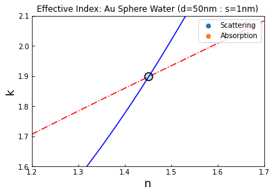
- Define a search space in both n and k (the real and imaginary components of refractive index) over which to search for a solution. Having iteratively computed the forward model over this range of n and k, the instance in which the values of scattering and absorption cross-sections both match their counterparts from the geometry in step 1 constitute the desired solution. Each iteration of step 2 will produce a plot similar to the one below, where each contour represents the possible solutions for scattering and absorption respectively, and thus their intersection gives the effective refractive index. This should then be repeated for each wavelength in the desired range. The example plot below describes a 50nm diameter Au sphere in water with an illumination wavelength of 400nm, using a 1nm thick artificial layer to emulate a -300mV applied potential.
Finite element models describing the optical response of charged nanoparticles can then be computed using this set of effective refractive indices, with a peripheral domain who's dimensions are more suitable for computation. If the indices were computed correctly there should be strong agreement between the numerical simulations and Mie theory results. The next challenge is in extending this method to more complex geometries.

