Difference between revisions of "Vlsi:Cadence Tips"
(Added diagrams to Voltage Storm analysis procedure.) |
|||
| Line 1: | Line 1: | ||
| + | === Tips with their own pages === | ||
| + | |||
| + | [[Vlsi:Cadence_Voltage_Storm]] | ||
| + | |||
=== Virtual Connections in Assura LVS === | === Virtual Connections in Assura LVS === | ||
| Line 6: | Line 10: | ||
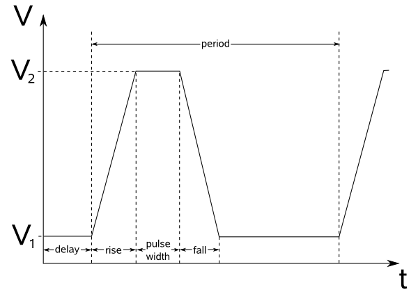
I can never remember which voltage/current is which, so I've created an image to remind me: [[Image:Vpulse.png]] | I can never remember which voltage/current is which, so I've created an image to remind me: [[Image:Vpulse.png]] | ||
| − | |||
| − | |||
| − | |||
| − | |||
| − | |||
| − | |||
| − | |||
| − | |||
| − | |||
| − | |||
| − | |||
| − | |||
| − | |||
| − | |||
| − | |||
| − | |||
| − | |||
| − | |||
| − | |||
| − | |||
| − | |||
| − | |||
| − | |||
| − | |||
| − | |||
| − | |||
== RC Extraction for C35/S35/H35 in IC 6.1 == | == RC Extraction for C35/S35/H35 in IC 6.1 == | ||
To run RCX successfully, you must first pass LVS correctly as normal. Do this by running LVS without any switches. If you run RCX now, it will fail. Now carry out LVS with the switch "resimulate_extracted" to guarantee that also substrate shorts are found correctly. RCX will run without any problems (note that you must not use the "resimulate_extracted" switch for normal LVS runs as it may give false results. | To run RCX successfully, you must first pass LVS correctly as normal. Do this by running LVS without any switches. If you run RCX now, it will fail. Now carry out LVS with the switch "resimulate_extracted" to guarantee that also substrate shorts are found correctly. RCX will run without any problems (note that you must not use the "resimulate_extracted" switch for normal LVS runs as it may give false results. | ||
Revision as of 17:31, 11 February 2009
Contents
Tips with their own pages
Virtual Connections in Assura LVS
If you have two wires on a layout that are unconnected but will be connected together in a higher level then place a pin on both wires. When running Assura LVS you need to set some further options. Enable "View avParameters" and then click "Modify avParameters...". Find the "joinPins" option, enable it ("Use in run") and set it to "Top". Click OK to close the avParameters window. Now enable "View Additional Functions" followed by "Use joinableNet Function". Now click "Modify joinableNet Function...". In the new window enable "root cell?" then add your net to the "Net Names to Join" box and click "Add to Command List (below)" to add it. Click OK to close the joinableNet window and then run LVS as normal.
Voltage / Current Pulse Sources
I can never remember which voltage/current is which, so I've created an image to remind me: 
RC Extraction for C35/S35/H35 in IC 6.1
To run RCX successfully, you must first pass LVS correctly as normal. Do this by running LVS without any switches. If you run RCX now, it will fail. Now carry out LVS with the switch "resimulate_extracted" to guarantee that also substrate shorts are found correctly. RCX will run without any problems (note that you must not use the "resimulate_extracted" switch for normal LVS runs as it may give false results.