Vlsi:Cadence Voltage Storm
From Applied Optics Wiki
Voltage Storm Analysis
Voltage Storm is a tool that allows the analysis of IR drops. For example, it can be used to monitor the distribution of VDD across an array of pixels. Follow this procedure for the analysis:
- Create your schematic and layout.
- Make sure your labels are in the center of any path or metal or poly they are on.
- From the Create menu, choose Pins from labels... and click OK to create pins on the layout. For AMS processes, the label that is on layer PIN M1 must have a pin on layer MET1 PIN and so on for all of the layers. Make sure you change these layers, or it won't work.
- Run LVS from Assura, and then run RCX to generate the extracted view. You may need to use the JoinableNet function if you haven't joined some nets together.
- In the RCX window, choose to extract R and use infinite Max Fracture Lengths squares in the Extraction tab, and enable extract parasitic resistor width (Netlisting Tab).
- Set up a test bench configuration, containing the extracted view. Use the hierarchy editor.
- Run a simulation that uses the extracted view. A short transient, AC or DC simulation is fine.
- From your Spectre ADE window, choose Session >> Schematic Window to open the test cell, and descend into the extracted view. This makes sure that you are in context.
- From the extracted view menu, choose Tools >> Voltage Storm from the menu.
- Select from the EM and IR menu, IR Drop Analysis
- Accept the use of the presistor (default)
- If all was correctly set up, your pins and available signals will be listed. Select the pins or signals of interest, using the CTRL key for multiple selections.
- Enter or browse to your simulation directory.
- Highlight one of the simulations in the list box.
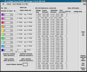
- Press OK. The tool will perform some operations (can be seen in the CIW), and an IR Voltage Drop Results window will pop up.
- This allows you to choose on of those pins/signals chosen earlier, and study the drop.
- To display the voltage distribution, click one of the buttons near the bottom of the form. Hide layers, Display highlights is particularly useful.
- It may be necessary to load a resource file in your LSW to get the layers to display in a nice format. From the LSW, choose Edit >> Resource Editor, and from that window choose File >> Load and load the display_vdrop.drf file.
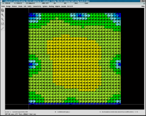
- The voltage variation is shown in the form of a colour map on the extracted layout window.

